Time Travel: How to Build a Precision Digital Clock with Arduino & DS3231
Stop using delay() for time! Learn to master the DS3231 Real Time Clock (RTC), I2C protocol, and CR2032 battery backups to keep precise time for years.
Read More →
* SYSTEM.NOTICE: Affiliate links support continued laboratory research.
Yesterday, we built Logic. We built a machine that could make a decision. “If A AND B, then Action.” But there was a flaw. A fatal flaw. As soon as you let go of the buttons… the decision vanished. The output died. The machine had Amnesia.
Imagine a computer with no memory. It could calculate 2 + 2 = 4, but the instant it finished, it would forget the “4”. It couldn’t browse the web, because it couldn’t remember which pixels were on the screen a millisecond ago. It would be useless.
Today, we fix that. Today, we teach the silicon to Remember.

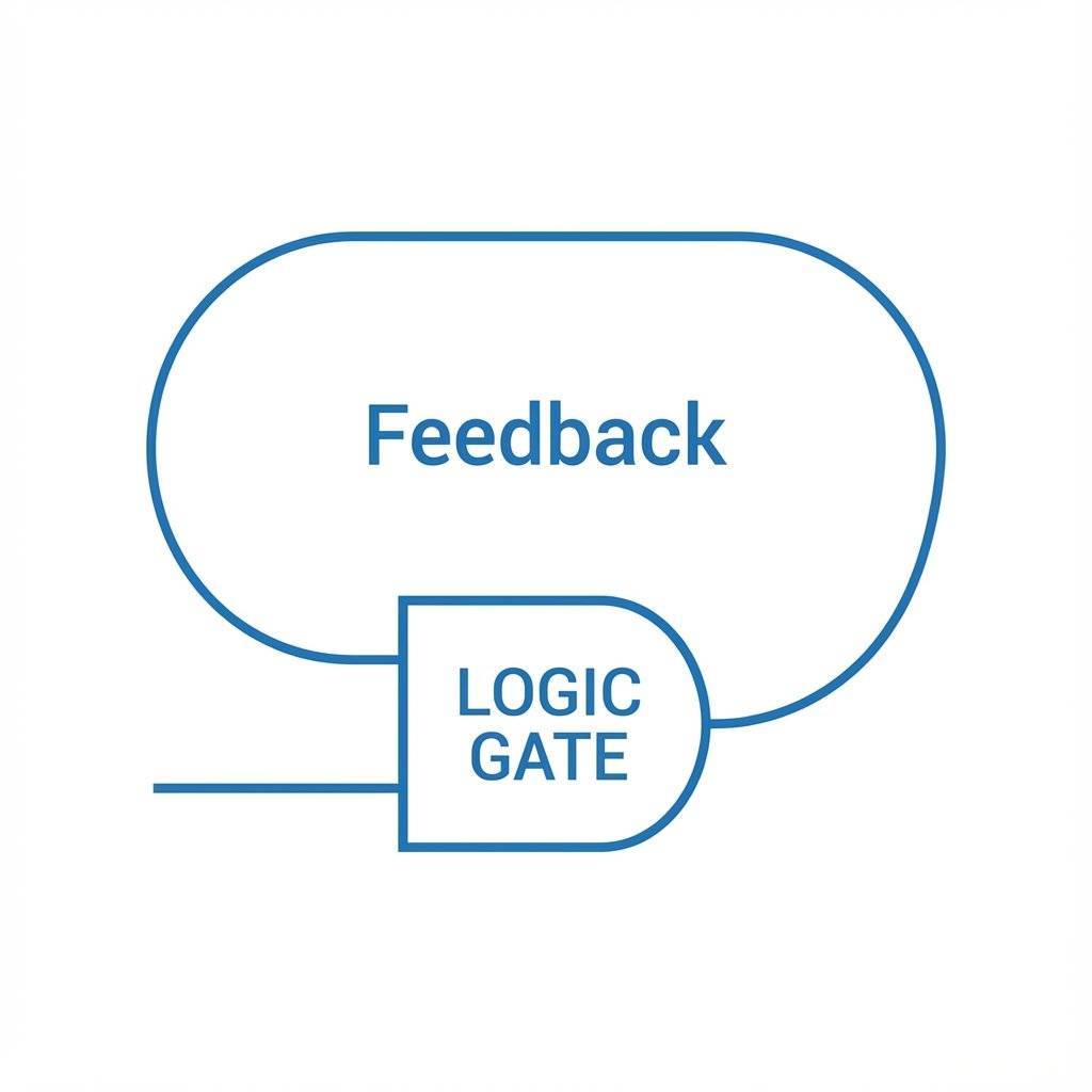
Logic gates (AND, OR, NOT) are “Combinational Logic.” Their output depends only on the current state of inputs. Input change -> Output change. Instantly. They have no sense of history. No “State”.
To create Memory, we need a circuit whose output depends on the Past. How do you make a circuit look backwards in time?
The secret is Feedback. You take the output of a gate, and you wire it back into its own input. It’s like looking in a mirror that reflects a mirror. Infinite loop. Or like a microphone pointed at a speaker—that screeching noise is the system feeding itself.
In a normal “Combinational” circuit (like an AND gate), the electrons flow in a straight line. River flows downstream. In a “Sequential” circuit (Memory), the river circles back. It becomes a whirlpool. Once the water starts spinning, it keeps spinning on its own momentum.
Positive Feedback allows a circuit to “lock” itself into a state and stay there.
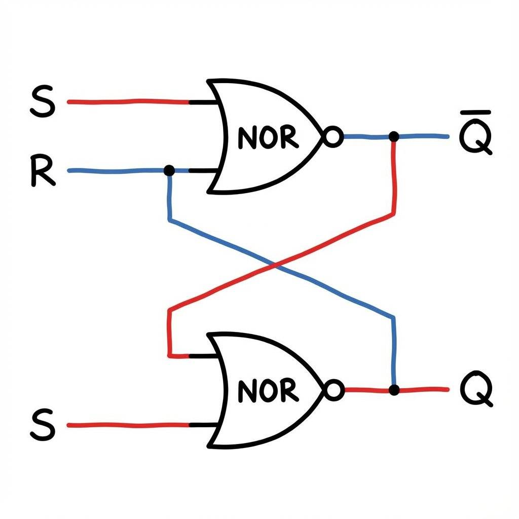
Let’s build the simplest possible memory cell. It’s called the SR Latch (Set-Reset Latch). We build it using two NOR gates (or NAND gates) connected in a cross pattern. Gate A’s output goes to Gate B’s input. Gate B’s output goes to Gate A’s input. They are locked in an eternal staring contest.
Imagine Gate A and Gate B. They are holding hands.
The value is trapped in the loop. It will stay trapped forever (as long as the battery lasts) until you hit RESET, which breaks the cycle and forces them to lock in the other direction.
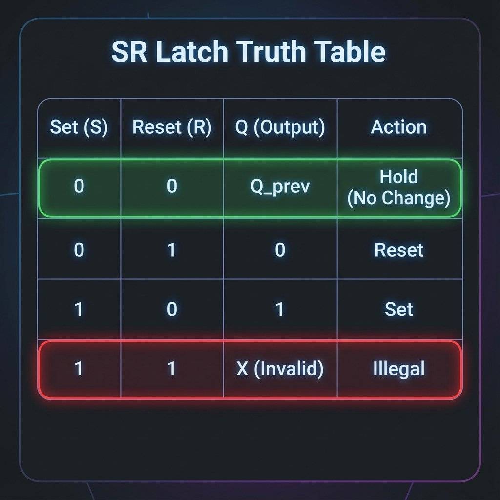
| Set (S) | Reset (R) | Action | Output (Q) |
|---|---|---|---|
| 1 | 0 | SET | 1 (On) |
| 0 | 0 | HOLD | Unchanged |
| 0 | 1 | RESET | 0 (Off) |
| 1 | 1 | ILLEGAL | Indeterminate |
Wait, what is “Illegal”? If you push Set and Reset at the same time, you are asking the circuit to be On and Off simultaneously. The Laws of Physics get confused. The gates fight. The output becomes unpredictable. In the digital world, unpredictability is death. Ideally, we want a chip that prevents us from doing this stupid thing.
Before we look at the better chip, we need to address a harsh reality of physics. You think when you press a button, it makes contact once. Click.
Wrong. Inside the switch, two pieces of metal are slamming together. They are elastic. They bounce. Like a tennis ball dropped on the floor. Click-clack-click-clack-click.
To a human, it feels like one press. To a chip that operates at 10,000,000 times a second, it looks like you pressed the button 50 times in 1 millisecond.
If you use a simple latch as a counter (1, 2, 3…), one button press might count as 17. This is called Switch Bounce.
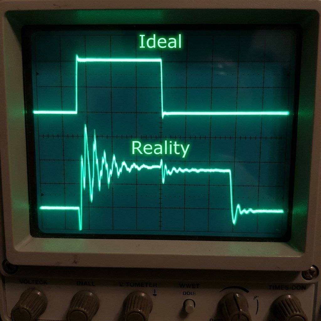
We need a bouncer at the club door. We need to ignore the jittery “noise” and only let the clean signal through. There are two ways:
We use a Capacitor and a Resistor (RC Circuit).
For today, we will skip the capacitor and rely on the “Clock” of the Flip-Flop to help us (mostly). But know this: All mechanical switches lie.
The SR Latch is crude. It has an illegal state. It’s asynchronous (uncontrolled). Enter the D Flip-Flop (Data Flip-Flop).
It adds two massive improvements:
You can change D all you want. Dance on the button. The output (Q) will not change. Only when the Clock goes from Low to High (Transition), the chip takes a “Snapshot” of D and copies it to Q. It filters out the noise between keypresses. It creates order.
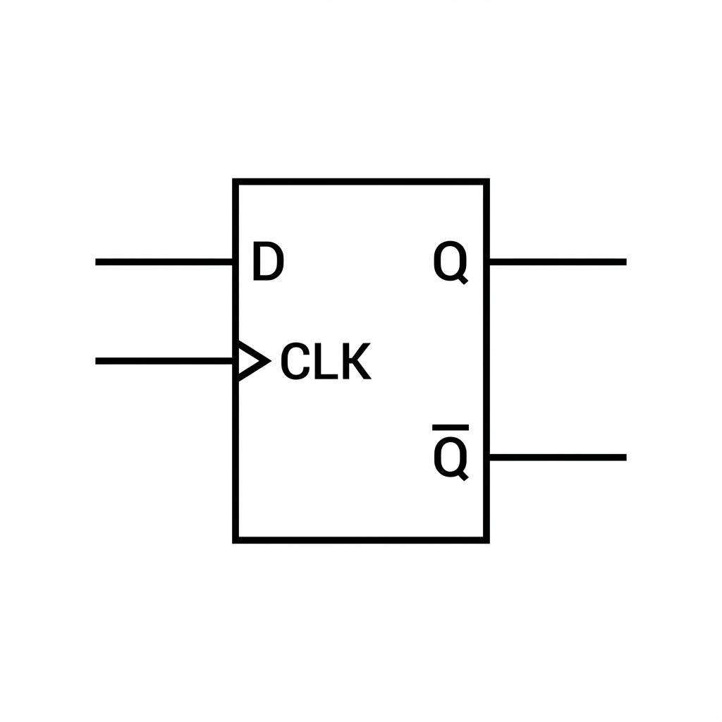
THIS is the building block of RAM. Your 16GB RAM stick is essentially 137 billion tiny D Flip-Flops and capacitors packing data.
It’s onomatopoeia. In early discrete transistor circuits, you could actually hear the relay click from one state to another. Flip… Flop… Flip… Flop. The name stuck. It sounds silly, but it describes the bistable action perfectly. It flips to 1, or flops to 0.
What happens if data arrives exactly at the same nanosecond the clock fires? The chip gets confused. It enters a state called Metastability. The output might hover at (halfway) for a few milliseconds before randomly picking 0 or 1. This is a nightmare for CPU designers. To prevent this, we must obey two rules found in the datasheet:
You might wonder, “What is actually inside the 74HC74?” Is it magic? No. It is just logic gates. 6 NAND gates, to be precise.
If you really wanted to, you could build a D Flip-Flop using the chips from Day 7 (NAND gates). It uses a clever arrangement called the Master-Slave configuration.
This complexity is why we buy the chip. Building one D Flip-Flop takes 6 NAND gates (1.5 chips). Building a 4-bit counter would take 6 chips and a spaghetti monster of wires. The 74HC74 gives you two of them for 50 cents.
On Day 4, we learned that transistors are switches. Can’t we just wire two transistors back-to-back to store data? Yes. This is called a Bi-Stable Multivibrator.
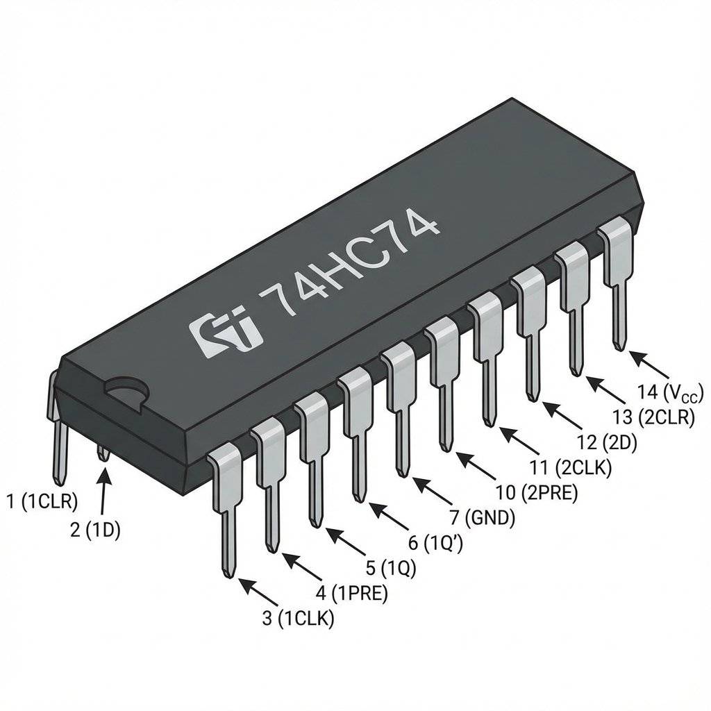
Pinout Breakdown:
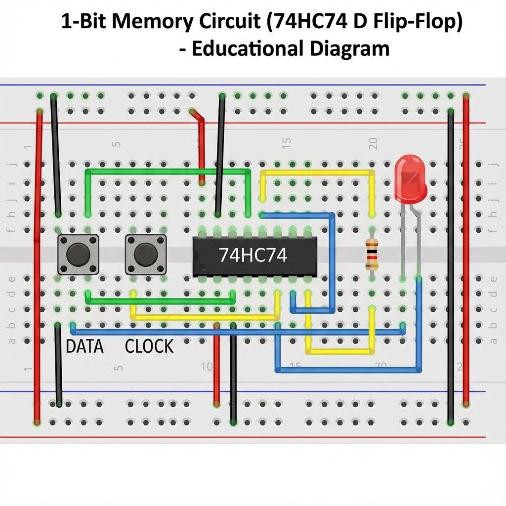
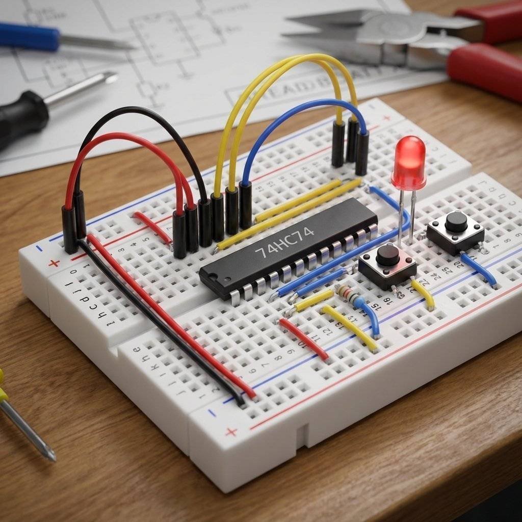
We are going to build a machine that “Saves” the state of a button.
If you press Button A: Nothing happens. The LED ignores you. If you HOLD Button A and tap Button B: Snap. The LED turns ON. Now you can release Button A. The LED stays ON. It remembers that you were pressing A when the photo was taken.
This looks complex, but follow the wires one by one.
Critical Wiring Details:
System Status: You have trapped a “1”.
System Status: You trapped a “0” (because A was 0 when you clocked).
It works exactly like a camera. Button B is the Shutter. Button A is the Scene. The film (Q) only changes when the Shutter clicks.
Before you power up, quadruple check these:
To build the memory cell, you need:
| Component | Quantity | Specs | Notes |
|---|---|---|---|
| 74HC74 | 1 | Dual D-Flip Flop | The Core Brain |
| Push Button | 2 | Momentary Tactile | 1 for Data, 1 for Clock |
| LED | 1 | Red or Green | To see the output |
| Resistor | 1 | Current Limiting | |
| Resistor | 3 | Pull-Down / Pull-Up | |
| Power | 1 | 5V Source | USB or 3xAA |
| Breadboard | 1 | Size doesn’t matter | - |
Before chips like the 74HC74, how did computers remember? In the 1950s and 60s (including the Apollo Mission), they used Magnetic Core Memory. Imagine a woven blanket of copper wires. At every intersection, there was a tiny donut made of ferrite (iron).
To read a bit, you had to try to flip the magnet. If it flipped, you knew it was a 1. If it didn’t, it was a 0. This “Destructive Read” meant the computer had to immediately write the data back after reading it! It was heavy. It was expensive. It was woven by hand by seamstresses. But it was Non-Volatile. If the power went out, the magnets stayed magnetized. Today, we can store gigabytes in a chip the size of a fingernail, but we should respect the donut-weavers who got us to the moon.
You just built SRAM (Static RAM).
This is why your computer needs a hard drive (SSD). SSDs use Floating Gate Transistors (Flash Memory) which physically trap electrons in a cage of glass. They stay there for years without power. But Flash is slow. So computers use both:
Proof of understanding. Can you modify your “1-Bit Recorder” to be a “Toggle Switch”? Goal: Press the button once -> LED ON. Press again -> LED OFF. (Like a real light switch). Hint: You need to connect the Q-Bar output back to the D input. Every time the clock fires, it loads the inverse of what it currently is. If it’s ON, it loads OFF. If it’s OFF, it loads ON. Try it. It’s magic.
LED Flickers? Switch bounce! We simplified the clock button. In a pro circuit, we would add a capacitor to Button B to smooth the signal.
Reset Randomly? Check Pins 1 and 4. They MUST be connected to +5V. If they float, they pick up ghosts.
Nothing Happens? Did you confuse D and CLK? D prepares the value, CLK saves it.
Think about what defines “You”. Is it your logic? Your ability to make decisions? Or is it your memory? Your history? Without memory, logic is hollow. It reacts, but it cannot learn. Today, you gave your circuits a soul. You gave them a past. By trapping that single electron in a loop, you created a machine that exists in time, not just in the moment. That is profound.
One bit of memory is cool. But what if we chain them? What if the output of Flip-Flop A triggers Flip-Flop B? A -> B -> C -> D.
That is a Binary Counter. Tomorrow, on Day 9, we will chain these chips together to teach our machine to Count. We will build a 4-bit Binary Counter that counts from 0 to 15. From there, it’s a short hop to building a clock, a timer, and eventually… a CPU. The complexity is ramping up. But so is the fun.
Keep that data safe. See you tomorrow.

Stop using delay() for time! Learn to master the DS3231 Real Time Clock (RTC), I2C protocol, and CR2032 battery backups to keep precise time for years.
Read More →
KITT is calling. Learn how to build the legendary 'Knight Rider' scanning light effect using the CD4017 Decade Counter and a 555 Timer.
Read More →
1, 2, 4, 8... Learn the secret language of computers. We demystify Binary, explain the Ripple Counter, and build a 4-bit machine using the 74HC93 chip.
Read More →