Why do we design PCBs? It’s not just about aesthetics.
Open EasyEDA Editor. We need to replicate our Day 31 Smart Home Hub.
Search for these specific LCSC Part Numbers or generic terms:
- NodeMCU V3: The brain.
- Relay: SRD-05VDC-SL-C.
- Transistor: 2N2222 (Switch).
- Diode: 1N4007 (Protection).
- OLED: SSD1306 I2C.
- Headers: 2.54mm Female.
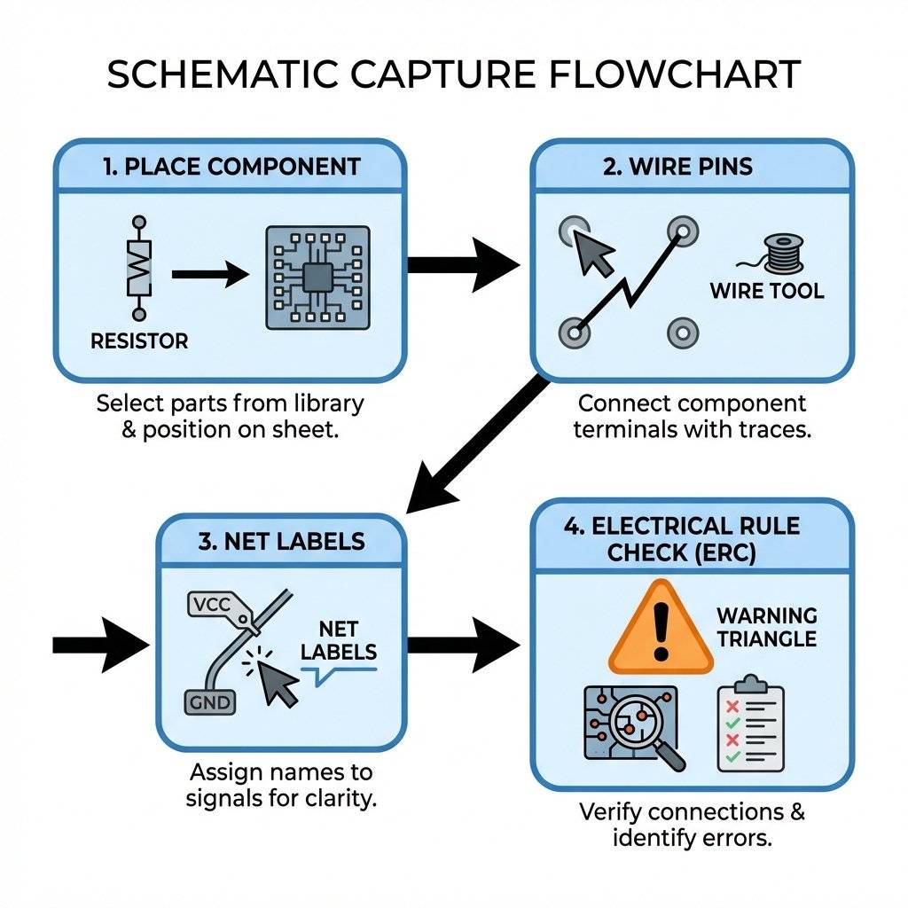
Critical Engineering Rule:
-
Net Labels: Keeps the schematic clean.
-
NetPorts: Dedicated VCC and GND symbols.
-
Labels: SDA, SCL, RELAY_SIG.
-
Why? This keeps the schematic readable. If you connect a label SDA to the OLED and SDA to the ESP8266, the software knows they are connected.
In a schematic, a resistor is a squiggly line. In the real world, it can be a tiny 1mm chip (0402) or a big 5-watt ceramic block.
-
The Symbol: The logical representation (Pin 1 to Pin 2).
-
The Footprint: The physical land pattern (Copper pads on the board).
Critical: EasyEDA lets you pick a generic “Resistor” symbol. If you don’t assign a Footprint, you can’t build the board.
-
Best Practice: Always select parts from the “LCSC Library”. These come with a Symbol, a Footprint, AND a 3D Model linked together.
-
Verification: Press Space on a component to rotate it. Double-click to check its “Package” attribute. If it says None or AXIAL-0.4 when you wanted 0805, fix it now.
The “Netlist” and Electrical Rules Check (ERC)
When you finish drawing, the software generates a Netlist.
This is a text file that lists every connection:
NodeMCU.Pin.D1 <--> OLED.Pin.SCL
NodeMCU.Pin.D2 <--> OLED.Pin.SDA
Run the ERC (Electrical Rules Check):
Before moving to layout, click Design -> Check DRC/ERC.
It catches errors like:
-
Floating Inputs: Pins that go nowhere.
-
Short Circuits: VCC touching GND.
-
Rule: 0 Errors, 0 Warnings. Do not ignore warnings.
Converting to PCB (The Physical Map)
Click “Convert Project to PCB”.
You will see a black screen with a jumble of components connected by thin blue “Ratlines”.
These lines represent the connections you need to make.
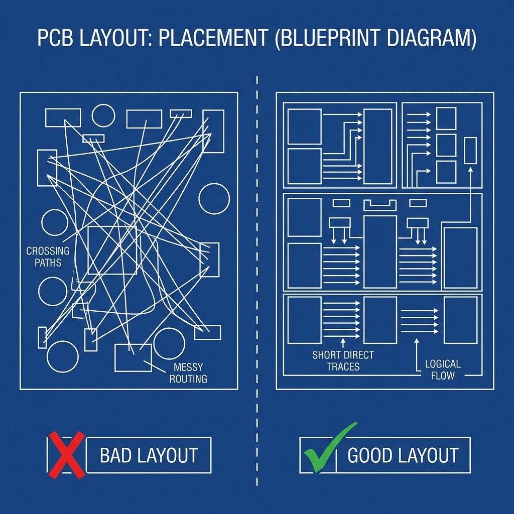
Component Placement Strategy
This is an art form.
-
Place Connectors First: USB ports, screw terminals, and headers should be on the edge of the board.
-
Core Components Center: The NodeMCU goes in the middle.
-
Keep Paths Short: Rotate the OLED and Relay so their pins face the NodeMCU pins they connect to.
Bad: Relay pin facing North, ESP pin facing South (Trace has to loop around).
- Good: Relay pin facing South, ESP pin facing South (Direct line).
Defining the Board Outline
Select the “BoardOutLine” layer (Pink). Draw a rectangle around your components.
-
Constraint: Make it small to save money, but leave breathing room for screws.
-
Mounting Holes: Place four 3mm holes in the corners for M3 screws.
Routing (Drawing the Traces)
Now we replace the “Ratlines” with real Copper Traces.
Select “Route” -> “Track”.
Trace Width Physics (IPC-2221)
How wide should a line be? It’s physics.
Current flows through copper → copper has resistance → resistance creates heat (I2R).
-
Signal Traces (Data): 0.254mm (10 mil). These carry almost zero current (micro-amps). Thin is fine.
-
Power Traces (5V, GND, Relay Coil): 0.5mm - 1.0mm.
-
The Calculation:
1 Amp current.
-
1oz Copper (Standard thickness: 35 micrometers).
-
Allowed Temp Rise: 10°C.
-
Result: You need at least 0.3mm (12 mil). We use 0.5mm for safety.
-
Why? If you pull 1 Amp through a hair-thin trace (6 mil), it will heat up, delaminate from the fiberglass, and burn (Fusing Current).
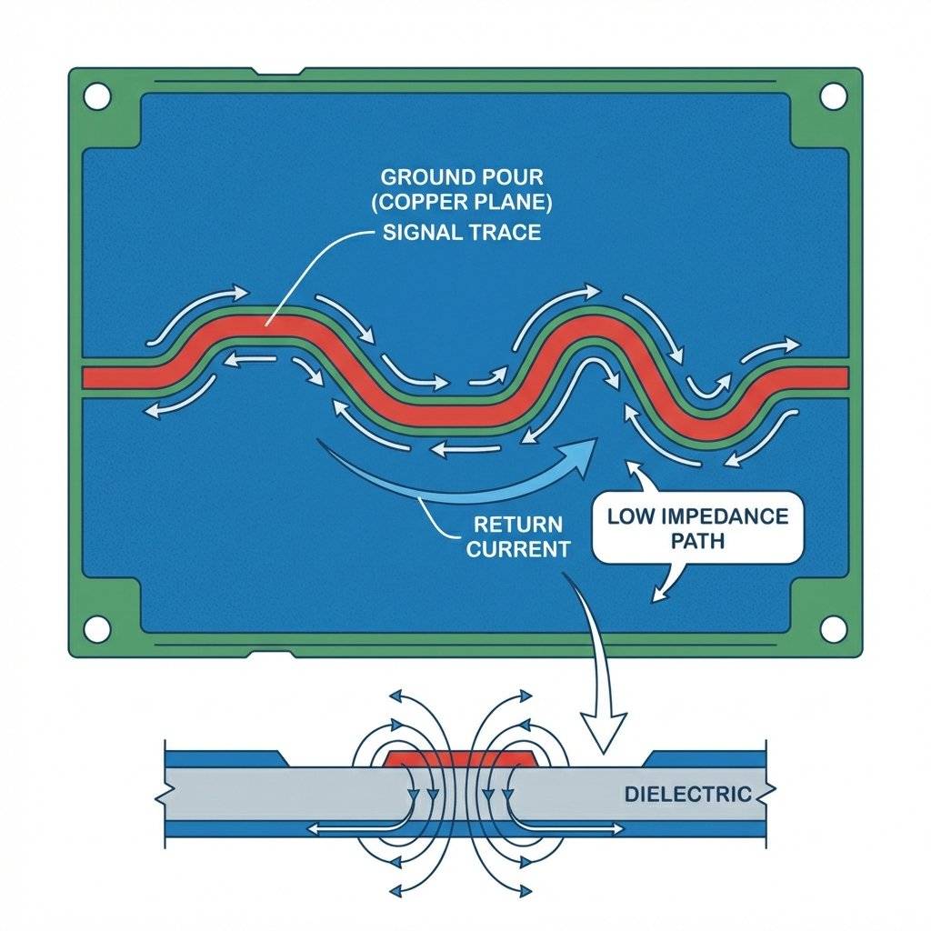
Pro Tip: Use a Ground Plane (Copper Pour).
Instead of routing Ground wires, we pour copper over the entire unused space of the board and connect it to GND.
-
Select “Copper Area”.
-
Assign Net: GND.
-
Draw a box around the whole board.
-
Benefit 1: Low Impedance Return Path. Current wants to return to the source via the path of least impedance. A giant sheet of copper is near-zero impedance.
-
Benefit 2: EMI Shielding. The ground plane acts as a faraday cage, absorbing stray RF noise.
-
Benefit 3: Cooling. The entire board acts as a heatsink.
Vias: The Elevators
We have a 2-Layer board (Top and Bottom).
Sometimes tracks cross. You cannot cross two tracks on the same layer.
The Solution: A Via.
It is a drilled hole (typically 0.4mm diameter) plated with copper that connects the Top Layer to the Bottom Layer.
- Rule of Thumb: Minimize vias; each adds impedance.
- High Current: Use multiple vias for power paths.
The Return Path (Advanced)
For DC, current takes the path of least resistance.
For High Frequency (Wi-Fi 2.4GHz), current takes the path of Least Inductance.
This means the return current on the Ground Plane will hug directly underneath the signal trace on the top layer.
Critical Rule: Do not cut your Ground Plane!
If you run a long track on the bottom layer that slices the Ground Plane in half, the return current has to take a huge detour loop. This creates a Loop Antenna, radiating noise and ruining your Wi-Fi signal.
Keep your Ground Plane solid.
Decoupling Capacitor Physics
You will see 100nF (0.1uF) capacitors next to every microchip power pin.
V=L⋅dtdi
Crystal Routing (Differential Pairs)
If you design a standalone ESP8266, you have a 26MHz Crystal.
-
Length Matching: The two tracks (XTAL_IN, XTAL_OUT) must be exactly the same length.
-
Guard Ring: Surround these tracks with Ground Vias to shield them from noise.
-
Why? If the clock signal is jittery, your Wi-Fi will fail to connect.
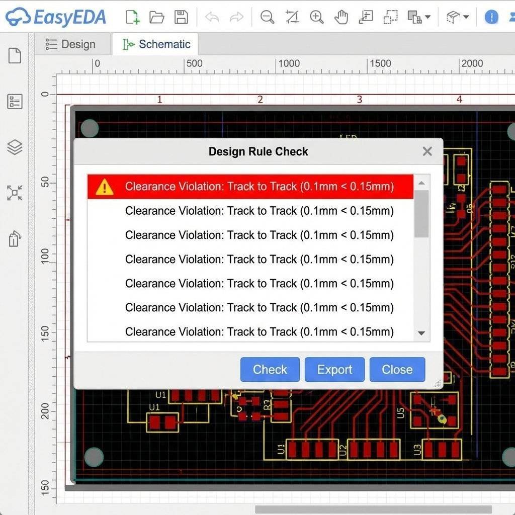
Design Rule Check (DRC)
Before you manufacture, you must run the DRC.
This checks your board against the factory’s capabilities (JLCPCB rules).
If you put two tracks 0.01mm apart, the factory cannot etch that. They will short circuit.
The DRC will flag this with a big red “X”. Fix every single error.
Manufacturing (The Anatomy of a PCB)
The factory doesn’t want your EasyEDA project file. They want Gerber Files.
A Gerber file is like a PDF for machines. It tells the laser diagram plotter exactly where to draw.
The Layers Explained
When you hold a PCB, you are looking at a sandwich:
-
Silkscreen (White): The text. SilkTop.gbr. Purely for humans.
-
Solder Mask (Green): The protective lacquer. MaskTop.gbr. It prevents solder bridges and protects copper from oxidation.
-
Copper (Shiny): The actual conductive path. TopLayer.gbr and BottomLayer.gbr.
-
Substrate (FR4): The yellow fiberglass body. Non-conductive.
Surface Finish: HASL vs ENIG
You will be asked to choose a finish.
- HASL (Hot Air Solder Leveling): Cheap and robust.
- ENIG (Electroless Nickel Immersion Gold): Flat and oxidation resistant.
Pros: Perfectly flat, oxidation resistant, looks premium.
Export Steps:
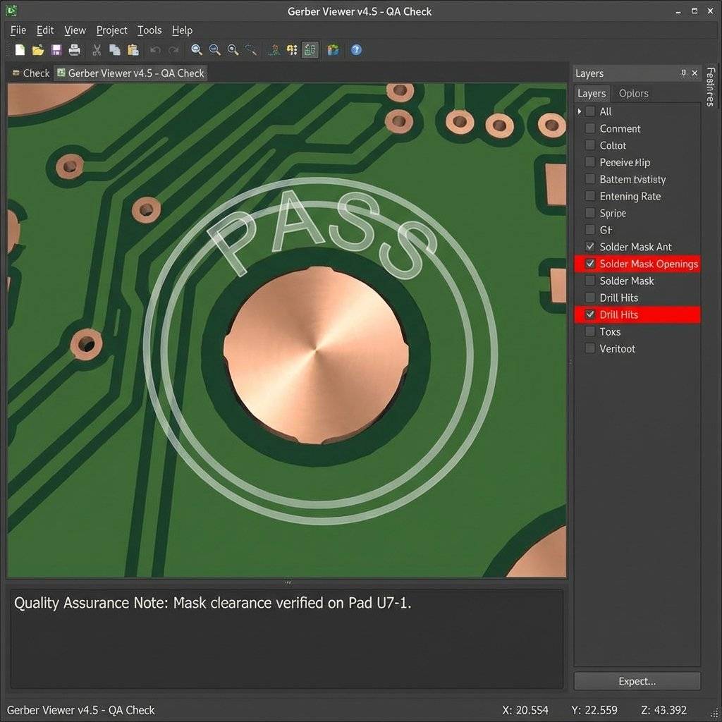
Check: Do you have Solder Mask openings over your pads? (If not, you can’t solder them).
- Check: Is the Silkscreen overlapping a drill hole? (The drill will obliterate the text).
The Bill of Materials (BOM)
| Component | Package | Quantity | Purpose |
|---|
| NodeMCU | DIP-30 | 1 | The brain. |
| 5V Relay | SRD-05VDC | 1 | High-voltage switch. |
| 2N2222 Transistor | TO-92 | 1 | Relay driver. |
| 1N4007 Diode | DO-41 | 1 | Flyback protection. |
| 1k Resistor | 0805 | 2 | Current limiting. |
| Screw Terminal | 5.08mm | 2 | Power & load. |
Component Selection Strategy: 0805 vs 0603
When browsing LCSC, you see resistor sizes: 0402, 0603, 0805, 1206.
- 0402: Dust specs. Manual assembly near impossible.
- 0603: Industry standard. Solderable with practice.
- 0805 (Recommended): Perfect for beginners.
- 1206: Large; good for high-power resistors (0.25W+).
Capacitor Voltage Rating:
Always choose a voltage rating 2x your operating voltage.
- For a 5V circuit, do not buy a 6.3V capacitor. It will degrade. Buy at least 10V or 16V.
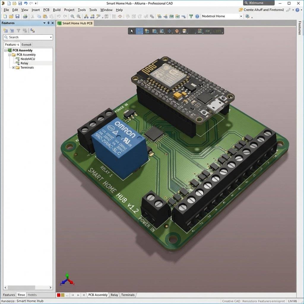
3D Visualization
One of the coolest features of modern EDA tools is the 3D View.
Click “3D View”. You will see a photorealistic render of your board.
Look closely at:
-
Component Height: Will the Relay block the USB port?
-
Silkscreen: Is the text “5V” readable, or is it under a resistor?
-
Physical Clash: Are the screw terminals facing outwards? (Common newbie mistake: Putting terminals facing inwards so you can’t put wires in).
The “Collision Check” Checklist
Before you order, perform this physical audit:
-
USB Port Clearance: Plug a real USB cable into your NodeMCU. Measure the plastic head width. Does it hit the Relay?
-
Screw Head Diameter: An M3 screw has a head diameter of ~5.5mm. Do you have copper traces too close to the mounting hole? The screw head will scrape the solder mask and short the trace to the case.
-
Tall Components: The Relay is 20mm tall. If you put this board in a 15mm slim case, the lid won’t close.
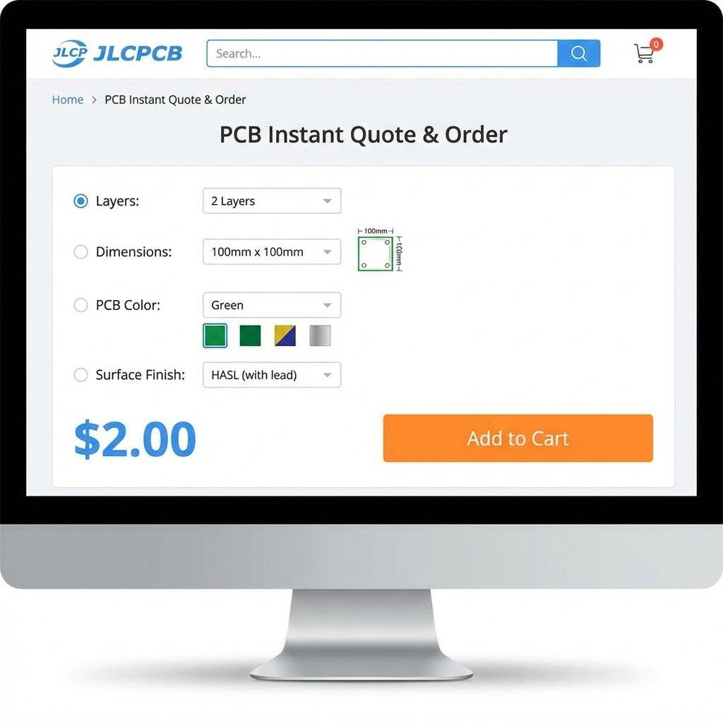
Ordering the Board
You go to a manufacturer (JLCPCB, PCBWay, OSHPark).
-
Upload the Gerber ZIP.
-
Select Settings:
Layers: 2.
-
Dimensions: (Auto-detected).
-
PCB Thickness: 1.6mm (Standard).
-
PCB Color: Green (Fastest), Black (Coolest, but harder to trace debug), Blue, Red.
-
Surface Finish: HASL (Solder) or ENIG (Gold - flatter, expensive). For DIY, HASL is fine.
-
Price: Usually $2 for 5 boards + Shipping.
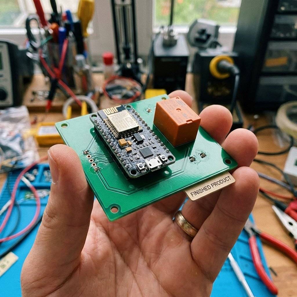
Wait 1 Week.
When the package arrives, you have graduated. You hold in your hand a fiberglass/copper sandwich that you designed.
Troubleshooting Common PCB Mistakes
Even pros make mistakes. Here are the “Big Three” to avoid:
The Acid Trap
When two tracks meet at an acute angle (less than 90°), the etching acid gets trapped in the corner during manufacturing. It eats away the copper over time, causing an open circuit weeks later.
- The Fix: Always route traces at 45° angles. Never 90°. Never acute.
Tombstoning (SMD Only)
If one pad of a resistor has a massive copper trace (heatsink) and the other has a tiny trace, the massive one heats up slower during reflow. The solder melts on the small pad first, pulling the component upright like a tombstone.
- The Fix: Use “Thermal Relief” spokes on your Ground Pads. Don’t connect a pad directly to a solid plane.
The “Mirrored” IC
You place a connector on the bottom layer, but forget to mirror the pinout. Now VCC connects to GND.
- The Fix: Print your PCB design on paper at 1:1 scale. Place your physical components on the paper. Does everything match?
Frequently Asked Questions (FAQ)
Q: Why not use KiCad?
A: KiCad is excellent and Open Source. However, for a beginner, the learning curve is steep. EasyEDA handles the Library and LCSC integration seamlessly, removing friction. Once you master PCB concepts, switching to KiCad is easy.
Q: Can I mill this on a CNC at home?
A: Yes, but it is messy (fiberglass dust is dangerous) and lacks Plated Through Holes (Vias). For $2, the factory quality is unbeatable.
Q: What is the “Silkscreen” limit?
A: Most cheap fabs can’t print text smaller than 0.8mm high. If you go smaller, it becomes a blurry blob.
Q: My board arrived and it doesn’t work. Why?
A: Did you run the DRC? Did you verify the Netlist? 99% of errors are in the Schematic. If the generic netlist says Pin 1 connects to Pin 2, the PCB software will force you to do it, even if it’s wrong electrically.
Conclusion & Next Steps
We have moved from “Does it work?” to “Is it manufacturable?”.
You now possess the skill to create custom hardware.
Next Steps:
-
SMD Soldering: We focused on Through-Hole (THT) mostly. Next, try Surface Mount Devices (SMD) like 0805 resistors. They are tiny but cheaper.
-
Custom Microcontrollers: Instead of a NodeMCU module, design the bare ESP8266-12F chip directly onto your board (requires 3.3V LDO, USB-UART bridge logic).
-
High Power: Designing traces for 220V AC (Creepage and Clearance rules becomes critical).
Your Assignment: Design a “Shield” for the NodeMCU that holds the relay and OLED, eliminating all wires. Order it. Build it.
Copyright © 2026 TechnoChips. Open Source Hardware (OSHW).


